Please refer to Semiconductor Electronics Materials Devices and Simple Circuits Class 12 Physics Important Questions with solutions provided below. These questions and answers have been provided for Class 12 Physics based on the latest syllabus and examination guidelines issued by CBSE, NCERT, and KVS. Students should learn these problem solutions as it will help them to gain more marks in examinations. We have provided Important Questions for Class 12 Physics for all chapters in your book. These Board exam questions have been designed by expert teachers of Standard 12.
Class 12 Physics Important Questions Semiconductor Electronics Materials Devices and Simple Circuits
Very Short Answer Type Questions
Question. How does the resistance of a semiconductor change when heated ?
Answer. Resistance decreases.
Question. Can a slab of p-type semiconductor be physically joined to another n-type semi-conductor slab to form p-n junction ? Justify your answer.
Answer. No, a p-type semi-conductor slab cannot be physically joined with a n-type semi-conductor slab to produce a p-n junction.
If we physically join the two semi-conductor blocks, there will always be little microscopic gap between the slabs due to roughness of the surfaces.
Question. Why a pure semiconductor behaves like an insulator at 0° K ?
Answer. The main cause for the conduction of any semiconductor is the number of free electrons in it. The free electrons has the kinetic energy which depends upon the temperature. As the temperature is 0K, the kinetic energy will be zero and the free electrons are not available for conduction.
Question. Is ohm’s law obeyed for semiconductors?
Answer. In case of semiconductors, Ohm’s law is obeyed for low electric fields i.e., E less than 106 V/m. If the field is increased above this value, the current becomes independent of the voltage applied.
Question. Which charge carriers an intrinsic semiconductor will have conduction ?
Answer. Electrons and holes.
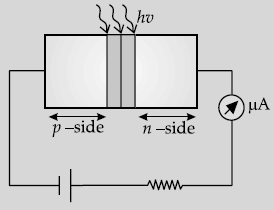
Question. What is the purpose of using photodiodes?
Answer. To detect optical signals.
Question. How does semiconductor behave in the presence of impurities?
Answer. When an impurity is added, the conductivity increases. As we know that conductivity is inversely proportional to resistivity, so the semiconductor does not behave like insulators even at 0K when an impurity atom is added to it.
Question. Does the width of a depletion region of a p-n junction vary if doping concentration is increased?
Answer. Width decreases.
Question. What is the name of the ability of a junction diode to convert an AC to DC based on the fact that it allows current to pass only when it is forward biased?
Answer. Rectification.
Question. Why is the energy gap much more in Silicon than in Germanium ?
Answer. The behaviour of semiconductor depends upon the extent of the energy gap between the valence band and conduction band. Thus, the valence electrons are quite tightly bound to the parent nuclei in case of Silicon as compared to Germanium.
Question. Will the presence of an intermediate band actually increase the fermi level or conventional semiconductor gap of that material?
Answer. The important requisites of an intermediate band is that it is not electronically coupled to the other bands, which means that one cannot have a single Fermi level. Instead, there should be the formation of three separated quasi-Fermi levels within the three bands i.e., conduction band, valence band and intermediate band.
Question. In half wave rectification, what is the output frequency if input frequency is 50 Hz.
Answer. Output frequency is 25 Hz.
Question. In a p-n junction diode, the forward bias resistance is low as compared to the reverse bias resistance. Give reason.
Answer. In a forward biased p-n junction, potential barrier is lowered and hence the electrons and holes can easily cross the junction. In reversed biased p-n junction, the potential barrier is raised and hence the electrons and holes cannot easily cross the junction. For this reason, forward bias resistance is low compared to reverse biased resistance of p-n junction.
Question. On which parameters do the wavelength and intensity of light emitted by an LED depend upon ?
Answer. Intensity depends on forward bias voltage and wavelength depends on energy gap of the semiconductor.
Question. Name the junction diode whose I-V characteristics is drawn below:
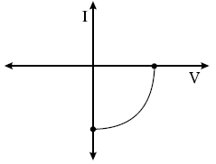
Answer. Solar cell
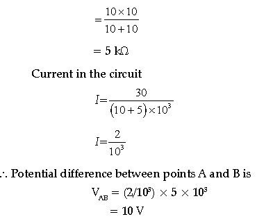
Question. In the given circuit, what is the potential difference between the A and B ?

Answer. Here p-n junction is forward biased. If p-n junction is ideal, its resistance is zero. The effective resistance across A and B
Question. Write the two processes involved in the formation of p-n junction.
Answer. (i) Diffusion
(ii) Drift
Question. The graph shown in the figure represents a plot of current versus voltage for a given semiconductor.
Identify the region, if any, over which the semiconductor has a negative resistance.

Answer. It is known that negative resistance is a property of an electrical circuits/devices where an increase in voltage across the device terminals results in decrease in electric current. From the graph, it is observed that region BC experiences negative resistance.
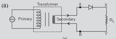
Question. Find the value of current through the resistor R of the circuits (i) and (ii) when similar diodes D1 and D2 are connected as shown in figure.

Answer. In figure (i), the diode D1 and D2 are forward biased
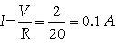
In figure (ii), D1 is forward biased but D2 is reverse biased due to which D2 offers infinite resistance
∴ I = 0
Short Answer Type Questions-I
Question. (a) Explain the formation of energy bands in crystalline solids.
(b) Draw the energy band diagrams of (i) a metal and
(ii) a semiconductor.
Answer. (a) Formation of energy bands in solid:
An isolated atom possesses discrete energies of different electrons. When two isolated atoms are brought very close to each other, the electrons in the orbits of two atoms interact with each other and the energies of electrons do not remain in same level but changes from its original value. So, at the place of each energy level, a closely spaced two energy levels are created.
When large number of atoms are brought together to form a solid by interaction of electrons, a large number of closely spaced energy levels is created. These are known as bands of allowed energies. Between the bands of allowed energies, there are empty energy regions also, known as forbidden band of energies.

Question. Write two points of difference between intrinsic and extrinsic semiconductors.
OR
Distinguish between ‘intrinsic’ and ‘extrinsic’ semiconductors.
Answer. Any two differences

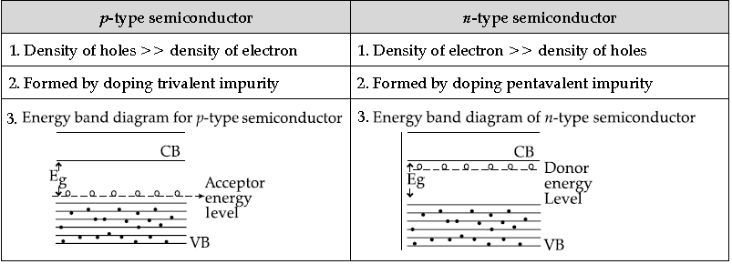
Question. Draw energy band diagrams of n-type and p-type semiconductors at temperature T > 0 K. Mark the donor and acceptor energy levels with their energies.
Answer.
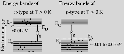
Question. Draw energy band diagram of p and n type semiconductors. Also, write two differences between p-type and n-type semiconductors.
Answer.
Question. Draw the energy band diagram when intrinsic semiconductor (Ge) is doped with impurity atoms of Antimony (Sb). Name the extrinsic semiconductor so obtained and majority charge carriers in it.
Answer. Well labelled energy band diagram of n-type semiconductor
n-type semiconductor
electrons-majority charge carriers
Question. (a) Why is a photodiode operated under reverse bias condition ?
(b) Draw V-I characteristic curves of photodiode for incident light of intensities I1 and I2 (I1 > I2).
Answer. (a) Photodiodes conduct in reverse biased condition only when a light of suitable frequency is incident on it. During reverse bias, the current is mainly due to the drift of minority charge carriers crossing the junction. The variation in intensity of light affects the minority charge carriers concentration and hence the reverse current is predominant.
In forward bias condition, the change in majority charge carriers is not much affected by light intensity and hence the forward current variation is not so predominant.
Hence, photodiodes are operated in reverse bias condition.

Question. (a) State the level of doping and biasing condition used in light emitting diode (LED).
(b) Write any two advantages of LED over the conventional low power lamps.
Answer. (a) LED is normally a heavily doped p-n junction diode. The doping level in LED determines the colour of light emitted.
LED is always operated in forward bias condition.
(b) Advantages of LED:
(i) LED has longer life span as compared to conventional lamps.
(ii) LED is extremely energy efficient device and may consume up to 90% less power than incandescent bulbs.
Question. Explain with help of circuit diagram, the action of a forward biased p-n junction diode which emits spontaneous radiation. State the least band gap energy of this diode to have emission in visible region.
Answer. Circuit diagram showing biasing of LED in forward bias Action of LED
For emission in visible range least band energy required is 1.8 eV
Question. Energy gap in a p – n photodiode is 2.8 eV. It can detect a wavelength of 6000 nm? Justify your answer.
Answer.

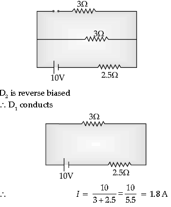
Question. Assuming that the two diodes D1 and D2 used in the electric circuit shown in the figure are ideal, find out the value of the current flowing through 2.5 Ω resistor.

Answer. In the circuit, if D1 is open and D2 is short, then equivalent circuit will result as:
Short Answer Type Questions-II
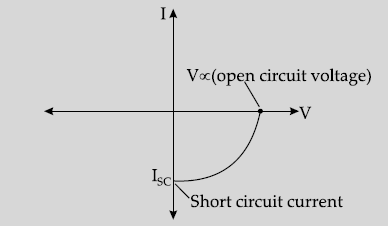
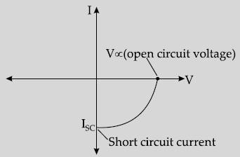
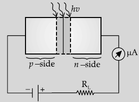
Question. What is a solar cell ? Draw V-I characteristics. Explain the three processes involved in the working.
Answer. Solar cell: A solar cell is an electrical device that converts the energy of light directly into electricity by the photovoltaic effect. Solar cell is a p-n junction fabricated from silicon. The energy conversion consists of absorption of light (photon) energy producing electron–hole pairs in the p-n junction and charge carrier separation.
I-V Characteristics:
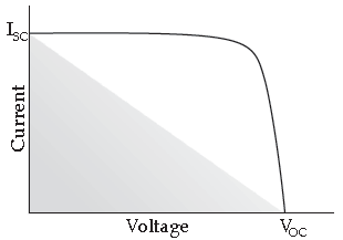
VOC: This is the maximum voltage that the PV array provides when the terminals are not connected to any load (an open circuit).
ISC: The maximum current provided by the PV array when the output connectors are shorted together (a short circuit condition).
Working of solar cell: A solar cell is a junction of n-type silicon and p-type silicon.
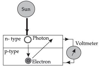
It generates electricity by using sunlight to make electrons move across the junction between the different types of silicon:
1. When sunlight shines on the cell, photons bombard the upper surface.
2. The photons carry their energy from n-type layer to p-type layer through p-n junction of the cell.
3. The photons transfer their energy to electrons in the p-type layer.
4. The electrons use this energy to move across the barrier into the n-type layer and flow out into the circuit.
5. This flow of electrons through the circuit gives rise to flow of current in the external circuit.
Question. Explain the information of potential barrier and depletion region in a p-n junction diode. What is effect of applying forward bias on the width of depletion region ?
Answer. Formation of depletion region: In the p-type semiconductor, holes are the majority carrier and in the n-type semiconductor, electrons are the majority carrier.
When a p-n junction is formed, some of the electrons from the n-region which have reached the conduction band are free to diffuse across the junction and combine with holes.
Filling a hole, makes a negative ion in p-side and a positive ion in the n-side. Thus, free charges get depleted and a depletion region is formed, which inhibits any further electron transfer.

Applying forward bias, the depletion region reduces and again electrons can diffuse.
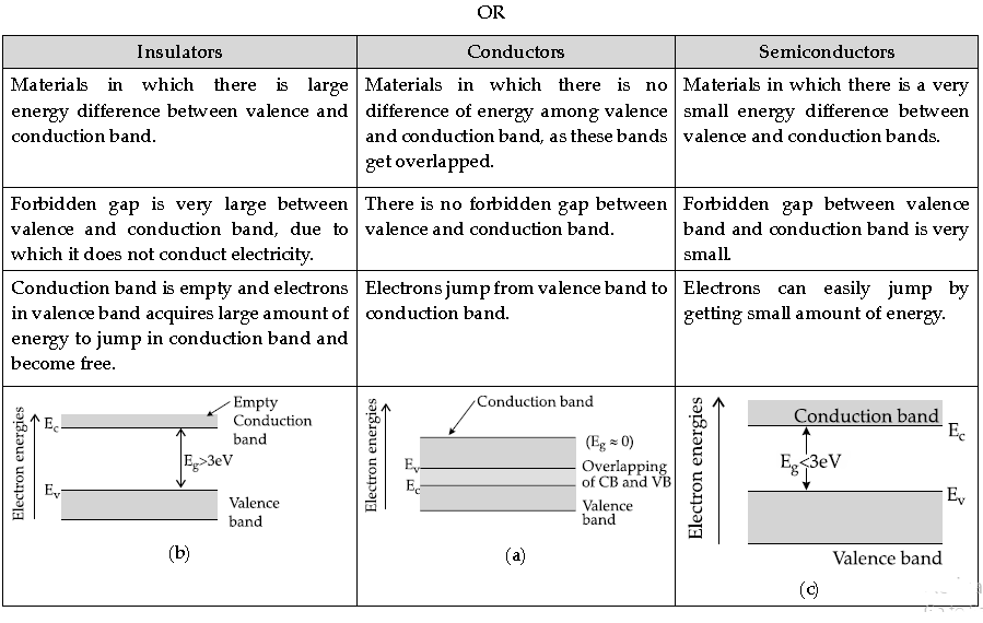
Question. Write any two distinguishing features between conductors, semiconductors and insulators on the basis of energy band diagrams.
Answer.

Two distinguishing features:
(i) In conductors, the valence band and conduction band tend to overlap (or nearly overlap), while in insulators they are separated by a large energy gap and in semiconductors, they are separated by a small energy gap.
(ii) The conduction band of a conductor has a large number of electrons available for electrical conduction. However, the conduction band of insulators is almost empty while that of the semi-conductor has only a (very) small number of such electrons available for electrical conduction.
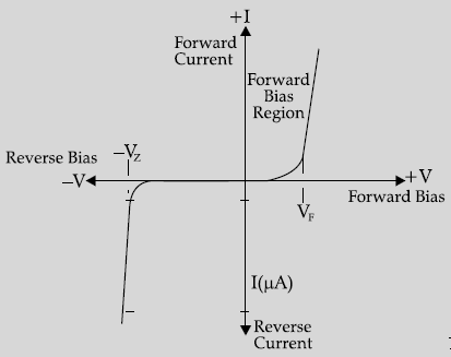
Question. Explain briefly with the help of necessary diagrams, the forward and the reverse biasing of a p-n junction diode. Also draw their characteristic curves in the two cases.
Answer. Circuit diagrams of p-n Junction under forward bias and reverse bias
Explanation of p-n junction working for forward and reverse bias
Characteristic curves for the two cases

In forward bias, applied voltage does not support potential barrier. As a result, the depletion layer width decreases and barrier height is reduced. Due to the applied voltage, electrons from n side cross the depletion region and reach p side. Similarly holes from p side cross the junction and reach the n side. The motion of charge carriers, on either side, give rise to current.
In reverse bias, applied voltage support potential barrier. As a result, barrier height is increased, depletion layer widens. This suppresses the flow of electrons from n → p and holes from p → n, thereby decrease the diffusion current. The electric field direction of the junction is such that if electrons on p side or holes on n side in their random motion comes close to the junction, they swept to its majority zone. This drift of carriers give rise to the current called reverse current.
Question. (a) In the following diagram, which bulb out of B1 and B2 will glow and why ?

(b) Draw a diagram of an illuminated p-n junction solar cell.
(c) Explain briefly the three processes due to which generation of emf takes place in a solar cell.
Answer. (a) Identification of the bulb and reason
(b) Diagram of solar cell
(c) Names of the processes
(a) Bulb B1 glows
Diode D1 is forward biased
(b) Diagram of solar cell:
(c) Three processes:
Generation
Separation
Collection
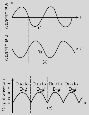
Question. Draw the circuit diagram of a full wave rectifier and explain its working. As so, give the input and output waveform.
Answer. Diagram of full wave rectifier : Working : The diode D1 is forward biased during one half cycle and current flows through the resistor, but diode D2 is reverse biased and hence no current flows through it. During the other half of the signal, D1 gets reverse biased and no current passes through it, D2 gets forward biased and current flows through it. In both half cycles current, through the resistor, flows in the same direction.
Question. Explain the two processes involved in the formation of a p-n junction diode. Hence define the term ‘barrier potential’.
Answer. Explanation of two processes Definition of barrier potential Diffusion: It is the process of movement of majority charge carriers from their majority zone (i.e., electrons from n ® p and holes from p → n) due to the electric field developed at the junction.
Drift: Process of movement of minority charge carriers (i.e., holes from n → p and electrons from p → n) due to the electric field developed at the junction.
Barrier potential: The loss of electrons from the n-region and gain of electrons by p-region causes a difference of potential across the junction, whose polarity is such as to oppose and then stop the further flow of charge carriers. This (stopping) potential is called Barrier potential
Question. State the reason, why the photodiode is always operated under reverse bias. Write the working principle of operation of a photodiode. The semiconducting material used to fabricate a photodiode, has an energy gap of 1.2 eV. Using calculations, show whether it can detect light of wavelength of 400 nm incident on it.
Answer. Reason for using in reverse bias
Working Principle
Whether it can detect
The fractional change, due to photo effects, on the minority charge carrier dominates reverse bias current, which is much more than the fractional change in the forward bias current and can be easily detected. Hence, photodiode is used in reverse
bias.
Working principle of photodiode:
(i) Generation of e-h pairs due to light close to junction.
(ii) Separation of electrons and holes due to electric field of the depletion region.
Detection is possible if Ep > Eg

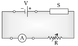
Question. (a) In the following diagram ‘S’ is a semiconductor. Would you increase or decrease the value of R to keep the reading of the ammeter A constant when S is heated ? Give reason for your answer.
(b) Draw the circuit diagram of a photodiode and explain its working. Draw its I/V characteristics.
Answer. (a) Correct Choice of R
Reason
(b) Circuit Diagram
Working
I-V characteristics
(a) R would be increased.
Resistance of S (a semiconductor) decreases onheating.
(b) Photodiode diagram
When the photodiode is illuminated with light (photons) (with energy (hn) greater than the energy gap (Eg) of the semiconductor), the electron-hole pairs are generated due to the absorption of photons. Due to junction field, electrons and holes are separated before they recombine. Electrons are collected on n-side and holes are collected on p-side giving rise to an emf.
When an external load is connected, current flows.
I-V Characteristics of the diode:

Question. Draw the I-V characteristic of an LED. State two advantages of LED lamps over conventional incandescent lamps. Write the factor which controls.
(a) wavelength of light emitted,
(b) intensity of light emitted by an LED.
Answer. I-V characteristics
Two advantages
Factors

Advantages (any two)
(i) Low operational voltage.
(ii) Less power consumption
(iii) Long life
(iv) Ruggedness [or any other]
(a) Energy band gap controls the wavelength of light emitted.
(b) Forward current controls the intensity of emitted light.
Question. (i) Explain with the help of a diagram the formation of depletion region and barrier potential in a p-n junction.
(ii) Draw the circuit diagram of a half wave rectifier and explain its working.
Answer. (i) Diagram of Formation
Explanation of formation of
Depletion region
Barrier potential
(ii) Circuit diagram of half wave rectifier
Explanation
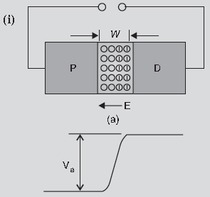
Due to diffusion and drift, the electrons and holes move across the junctions, creating a final stage in which a region is created across the junction wall, which gets devoid of the mobile charge carriers. This region is called depletion region; the potential difference across the region is called Barriers potential
Working- If an alternating voltage is applied across a diode in series with a load, a pulsating voltage will appear across the load only during that half cycle of the ac input during which the diode is forward biased.
Therefore, in the positive half – cycle of ac input there is a current through the load RL and we get an output voltage whereas half – cycle. There is no output during the negative half cycle. Thus, the output voltage is restricted to only one direction and is said to be rectified.
Question. With what considerations in view, a photodiode is fabricated ? State its working with the help of a suitable diagram. Even though the current in the forward bias is known to be more than in the reverse bias, yet the photodiode works in reverse bias. What is reason ?
Answer. It is fabricated with a transparent window to allow light to fall on diode.
When the photodiode is illuminated with photons of energy (hn > Eg) greater than the energy gap of the semiconductor, electron hole pairs are generated.
These get separated due to the junction electric field (before they recombine) which produces an emf.
Question. The graph of potential barrier versus width of depletion region for an unbiased diode is shown in (A). In comparison to (A), graphs (B) and (C) are obtained after biasing in diode in different ways. Identify the type of biasing in (B) and (C) and justify your answer.
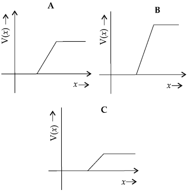
Answer. (i) In (B), the diode is reverse biased.
When a diode is reverse biased, the barrier height increase as the applied voltage increases since the free charge carriers (electrons and holes) are pulled apart from the junction by the applied voltage.
In (C), the diode is forward biased.
When a diode is forward biased, the barrier height decrease as the applied voltage increases since the free charge carriers (electrons and holes) are enabled to approach the junction by the applied voltage.
Long Answer Type Questions
Question. (a) Why are photodiodes preferably operated under reverse bias when the current in the forward bias is known to be more than that in reverse bias?
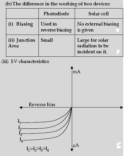
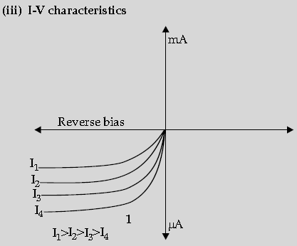
(b) The two optoelectronic devices: Photodiode and solar cell, have the same working principle but differ in terms of their process of operation. Explain the difference between the two devices in terms of (i) biasing, (ii) junction area and (iii) I-V characteristics.
Answer. (a) The fractional change in majority charge carriers is very less compared to the fractional change in minority charge carriers on illumination.