Please refer to MCQ Questions Chapter 14 Semiconductor Electronics Materials Devices and Simple Circuits Class 12 Physics with answers provided below. These multiple-choice questions have been developed based on the latest NCERT book for class 12 Physics issued for the current academic year. We have provided MCQ Questions for Class 12 Physics for all chapters on our website. Students should learn the objective based questions for Chapter 14 Semiconductor Electronics Materials Devices and Simple Circuits in Class 12 Physics provided below to get more marks in exams.
Chapter 14 Semiconductor Electronics Materials Devices and Simple Circuits MCQ Questions
Please refer to the following Chapter 14 Semiconductor Electronics Materials Devices and Simple Circuits MCQ Questions Class 12 Physics with solutions for all important topics in the chapter.
MCQ Questions Answers for Chapter 14 Semiconductor Electronics Materials Devices and Simple Circuits Class 12 Physics
Question. In germanium the energy gap is about 0.75 eV. The wavelength of light which germanium starts absorbing is
(a) 5000 Å
(b) 1650 Å
(c) 16500 Å
(d) 165000 Å
Answer
C
Question. A potential difference of 2 V is applied between the opposite faces of a Ge crystal plate of area 1 cm2 and thickness 0.5 mm. If the concentration of electrons in Ge is 2 × 10¹⁹/m3 and mobilities of electrons and holes are 0.36 m2 V–1 s–1 and 0.14 m2 V–1 s–1 respectively, then the current flowing through the plate will be
(a) 0.25 A
(b) 0.45 A
(c) 0.56 A
(d) 0.64 A
Answer
D
Question. Currents flowing in each of the following circuits A and B respectively are
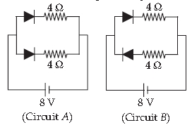
(a) 1 A, 2 A
(b) 2 A, 1 A
(c) 4 A, 2 A
(d) 2 A, 4 A
Answer
C
Question. The conductivity of a semiconductor increases with increase in temperature because
(a) number density of free current carries increases
(b) relaxation time increases
(c) both number density of carries and relaxation time increase
(d) number density of carries increases, relaxation time decreases but effect of decrease in relaxation time is much less than increase in number density
Answer
D
Question. A npn transistor is connected in common emitter configuration in a given amplifier. A load resistance of 800 W is connected in the collector circuit and the voltage drop across it is 0.8 V. If the current amplification factor is 0.96 and the input resistance of the circuit is 192W, the voltage gain and the power gain of the amplifier will respectively be:
(a) 4, 3.84
(b) 3.69, 3.84
(c) 4, 4
(d) 4, 3.69
Answer
A
Question. A p-n junction has acceptor impurity concentration of 1017 cm–3 in the P side and donor impurity concentration of 1016 cm–3 in the N side. What is the contact potential at the junction (KT = thermal energy, intrinsic carrier concentration ni = 1.4 × 1010 cm–3)?
(a) (KT/e) ln(4 × 10¹²)
(b) (KT/e) ln(2.5 × 10²³)
(c) (KT/e) ln(1023)
(d) (KT/e) ln(5 × 10¹²)
Answer
D
Question. A Zener diode has a contact potential of 1 V in the absence of biasing. It undergoes Zener breakdown for an electric field of 106 V/m at the depletion region of p-n junction. If the width of the depletion region is 2.5 mm, what should be the reverse biased potential for the Zener breakdown to occur?
(a) 3.5 V
(b) 2.5 V
(c) 1.5 V
(d) 0.5 V
Answer
B
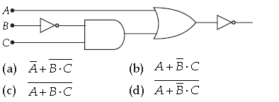
Question. If in a p-n junction, a square input signal of 10 V is applied as shown, then the output across RL will be
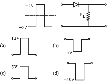
Answer
C
Question. In a semiconductor, separation between conduction and valence band is of the order of
(a) 0 eV
(b) 1 eV
(c) 10 eV
(d) 50 eV
Answer
B
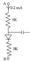
Question. A Zener diode, having breakdown voltage equal to 15 V is used in a voltage regulator circuit shown in figure. The current through the diode is
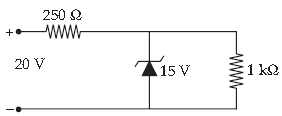
(a) 10 mA
(b) 15 mA
(c) 20 mA
(d) 5 mA
Answer
D
Question. To get output 1 for the following circuit, the correct choice for the input is
(a) A = 0, B = 1, C = 0
(b) A = 1, B = 0, C = 0
(c) A = 1, B = 1, C = 0
(d) A = 1, B = 0, C = 1
Answer
D
Question. Identify the logic gate from the following truth table:
Input Output
A B Y
0 0 1
0 1 0
1 0 0
1 1 0
(a) NOR gate
(b) NOT gate
(c) AND gate
(d) NAND gate
Answer
A
Question. In Boolean algebra, A⋅A is equal to
(a) A⋅B
(b) A+ B
(c) A ⋅ B
(d) A + B
Answer
D
Question. The given electrical network is equivalent to :
(a) OR gate
(b) NOR gate
(c) NOT gate
(d) AND gate
Answer
B
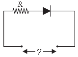
Question. In the given figure, a diode D is connected to an external resistance R = 100 Ω and an e.m.f. of 3.5 V. If the barrier potential developed across the diode is 0.5 V, the current in the circuit will be:

(a) 40 mA
(b) 20 mA
(c) 35 mA
(d) 30 mA
Answer
D
Question. The output from a NAND gate is divided into two in parallel and fed to another NAND gate. The resulting gate is a
(a) NOT gate
(b) AND gate
(c) NOR gate
(d) OR gate
Answer
B
Question. In a n-type semiconductor, which of the following statements is true?
(a) Electrons are minority carriers and pentavalent atoms are dopants.
(b) Holes are minority carriers and pentavalent atoms are dopants.
(c) Holes are majority carriers and trivalent atoms are dopants.
(d) Electrons are majority carriers and trivalent atoms are dopants.
Answer
B
Question. In the circuit shown in figure given below, if the diode forward voltage drop is 0.3 V, the voltage difference between A and B is

(a) 1.3 V
(b) 2.3 V
(c) 0
(d) 0.5 V
Answer
B
Question. The cause of the potential barrier in a p-n diode is
(a) depletion of positive charges near the junction
(b) concentration of positive charges near the junction
(c) depletion of negative charges near the junction
(d) concentration of positive and negative charges near the junction
Answer
D
Question. The gate for which output is high if atleast one input is low?
(a) NAND
(b) NOR
(c) AND
(d) OR
Answer
A
Question. Carbon, Silicon and Germanium atoms have four valence electrons each. Their valence and conduction bands are separated by energy band gaps represented by (Eg)C, (Eg)Si and (Eg)Ge respectively. Which one of the following relationship is true in their case?
(a) (Eg)C > (Eg)Si
(b) (Eg)C < (Eg)Si
(c) (Eg)C = (Eg)Si
(d) (Eg)C < (Eg)Ge
Answer
A
Question. Application of a forward bias to a p–n junction
(a) widens the depletion zone
(b) increases the potential difference across the depletion zone
(c) increases the number of donors on the n side
(d) increases the electric field in the depletion zone.
Answer
C
Question. The energy gap of silicon is 1.14 eV. The maximum wavelength at which silicon starts energy absorption, will be (h = 6.62 × 10⁻³⁴ Js ; c = 3 × 10⁸ m/s)
(a) 10.888 Å
(b) 108.88 Å
(c) 1088.8 Å
(d) 10888 Å
Answer
A
Question. The value of b
(a) is always less than 1
(b) lies between 20 and 200
(c) is always greater than 200
(d) is always infinity
Answer
B
Question. In a bridge rectifier, the number of diodes required is
(a) 1
(b) 2
(c) 3
(d) 4
Answer
D
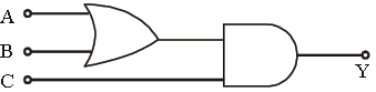
Question. The diagram of a logic circuit is given below. The output F of the circuit is represented by

(a) W . (X + Y)
(b) W . (X . Y)
(c) W + (X . Y)
(d) W + (X + Y)
Answer
C
Question. Hole in semiconductor is
(a) an anti – particle of electron
(b) a vacancy created when an electron leaves a covalent bond
(c) absence of free electrons
(d) an artificially created particle
Answer
B
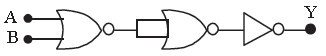
Question. The output Y of the logic circuit shown in figure is best represented as
Answer
D
Question. The resistance of a germanium junction diode whose V – I is shown in figure is (Vk = 0.3 V)

(a) 5 kΩ
(b) 0.2 kΩ
(c) 2.3 kΩ
(d) (10/2.3) kΩ
Answer
B
Question. To get an OR gate from a NAND gate, we need
(a) only two NAND gates.
(b) two NOT gates obtained from NAND gates and one NAND gate.
(c) four NAND gates and two AND gates obtained from NAND gates.
(d) none of these
Answer
B
Question. Mobilities of electrons and holes in a sample of intrinsic germanium at room temperature are 0.36 m2 V–1 s–1 and 0.17 m2 V–1 s–1. The electron and hole densities are each equal to 2.5 × 10¹⁹ m–3. The electrical conductivity of germanium is
(a) 4.24 S m–1
(b) 2.12 S m–1
(c) 1.09 S m–1
(d) 0.47 S m–1
Answer
B
Question. In a common emitter amplifier, the input signal is applied across
(a) anywhere
(b) emitter-collector
(c) collector-base
(d) base-emitter
Answer
D
Question. If in a triode valve amplification factor is 20 and plate resistance is 10 kΩ, then its mutual conductance is
(a) 2 milli mho
(b) 20 milli mho
(c) (1/2) milli mho
(d) 200 milli mho
Answer
A
Question. The output waveform of a full wave rectifier is
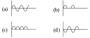
Answer
C
Question. A transistor is operated in common emitter configuration at VC = 2 V such that a change in the base current from 100 mA to 300 mA produces a change in the collector current from 10 mA to 20 mA. The current gain is
(a) 75
(b) 100
(c) 25
(d) 50
Answer
D
Question. For the given circuit of p-n junction diode, which of the following statements is correct?
(a) In forward biasing the voltage across R is V.
(b) In forward biasing the voltage across R is 2V.
(c) In reverse biasing the voltage across R is V.
(d) In reverse biasing the voltage across R is 2V.
Answer
A
Question. The amplification factor of a triode is 50. If the grid potential is decreased by 0.20 V, what increase in plate potential will keep the plate current unchanged?
(a) 5 V
(b) 10 V
(c) 0.2 V
(d) 50 V
Answer
B
Question. The current in the circuit will be

Answer
B
Question. In the circuit shown above, an input of 1 V is fed into the inverting input of an ideal Op-amp A. The output signal Vout will be

(a) +10 V
(b) – 10 V
(c) 0 V
(d) infinity.
Answer
B
Question. When a solid with a band gap has a donor level just below its empty energy band, the solid is
(a) an insulator
(b) a conductor
(c) p-type semiconductor
(d) n-type semiconductor.
Answer
D
Question. Zener diode is used for
(a) producing oscillations in an oscillator
(b) amplification
(c) stabilisation
(d) rectification
Answer
C
Question. In space charge limited region, the plate current in a diode is 10 mA for plate voltage 150 V. If the plate voltage is increased to 600 V, then the plate current will be
(a) 10 mA
(b) 40 mA
(c) 80 mA
(d) 160 mA
Answer
C
Question. Two identical p-n junctions are connected in series in three different ways as shown below to a battery. The potential drop across the p-n junctions are equal in

(a) circuits 2 and 3
(b) circuits 1 and 2
(c) circuits 1 and 3
(d) none of the circuit
Answer
A
Question. The temperature coefficient of a Zener mechanism is
(a) negative
(b) positive
(c) infinity
(d) zero
Answer
A
Question. The output stage of a television transmitter is most likely to be a
(a) plate-modulated class C amplifier
(b) grid-modulated class C amplifier
(c) screen-modulated class C amplifier
(d) grid-modulated class A amplifier
Answer
B
Question. In Colpitt oscillator the feedback network consists of
(a) two inductors and a capacitor
(b) two capacitors and an inductor
(c) three pairs of RC circuit
(d) three pairs of RL circuit.
Answer
B
Question. The conductivity of a semiconductor increases with increase in temperature because
(A) number density of free current carriers increases.
(B) relaxation time increases.
(C) both number density of carriers and relaxation time increase.
(D) number density of current carriers increases;
relaxation time decreases but decrease in relaxation time is much less than the increase in number density.
Answer
D
Question. A 220 V A.C. supply is connected between points A and B in Figure. What will be the potential difference V across the capacitor?
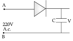
(A) 220 V
(B) 110 V
(C) 0 V
(D) 220 2 V
Answer
D
Question. The output of the given circuit in Figure
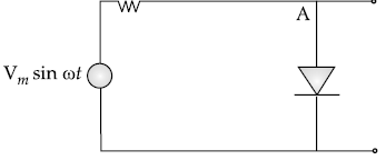
(A) would be zero at all times.
(B) would be like a half wave rectifier with positive cycles in output.
(C) would be like a half wave rectifier with negative cycles in output.
(D) would be like that of a full wave rectifier.
Answer
C
Question. Hole is
(A) an anti-particle of electron.
(B) a vacancy created when an electron leaves a covalent bond.
(C) absence of free electrons.
(D) an artificially created particle.
Answer
B
Question. In an n-type silicon, which of the following statement is true :
(A) Electrons are majority carriers and trivalent atoms are the dopants.
(B) Electrons are minority carriers and pentavalent atoms are the dopants.
(C) Holes are minority carriers and pentavalent atoms are the dopants.
(D) Holes are majority carriers and trivalent atoms are the dopants.
Answer
C
Question. Tetra valent semiconductor is to be doped with ____ valent element to achieve _____ type extrinsic semiconductor.
(A) penta, n
(B) tri, p
(C) penta, p
Answer
D
Question. In an unbiased p-n junction, holes diffuse from the p-region to n-region because
(A) free electrons in the n-region attract them.
(B) they move across the junction by the potential difference.
(C) hole concentration in p-region is more as compared to n-region.
(D) All of the above.
Answer
C
Question. The reverse saturation of p-n diode
(a) depends on doping concentrations
(b) depends on diffusion lengths of carriers
(c) depends on the doping concentrations and diffusion lengths
(d) depends on the doping concentrations, diffusion length and device temperature.
Answer
D
Question. When a forward bias is applied to a p-n junction, it
(A) raises the potential barrier.
(B) reduces the majority carrier current to zero.
(C) lowers the potential barrier.
(D) None of the above
Answer
C
Question. Carbon, silicon and germanium have four valence electrons each. These are characterised by valence and conduction bands separated by energy band gap respectively equal to (Eg )C ,(Eg )Si and (Eg )Ge Which of the following statements is true?
(A) (Eg )Si <(Eg )Ge <(Eg )C
(B) (Eg )C < (Eg )Ge > (Eg )Si
(C) (Eg )C > (Eg )Si > (Eg )Ge
(D) (Eg )C =(Eg )Si = (Eg )Ge
Answer
C
Question. Which one of the following diagrams depicts the proper flow or electrons and holes in a forward biased p-n junction diode?
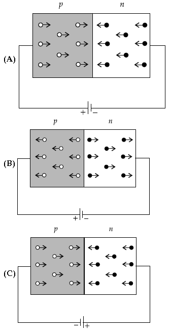
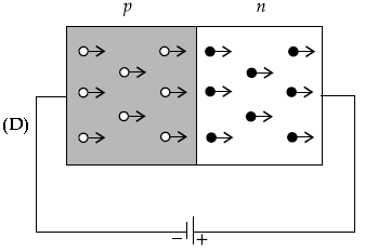
Answer
A
Question. Semiconductors behave like insulators at ______
(A) 0°C
(B) 0 K
(C) 273 K
(D) None of the these
Answer
B
Question. In Figure, Vo is the potential barrier across a p-n junction, when no battery is connected across the junction
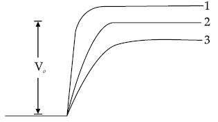
(A) 1 and 3 both correspond to forward bias of junction
(B) 3 corresponds to forward bias of junction and corresponds to reverse bias of junction
(C) 1 corresponds to forward bias and 3 corresponds to reverse bias of junction.
(D) 3 and 1 both correspond to reverse bias of junction.
Answer
B
Question. When the conductivity of a semiconductor is due to rupture of its covalent bond only then the semiconductor is called
(A) Intrinsic
(B) Extrinsic
(C) Donor
(D) acceptor
Answer
A
Question. In Figure, assuming the diodes to be ideal,
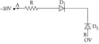
(A) D1 is forward biased and D2 is reverse biased and hence current flows from A to B
(B) D2 is forward biased and D1 is reverse biased and hence no current flows from B to A and vice versa.
(C) D1 and D2 are both forward biased and hence current flows from A to B.
(D) D1 and D2 are both reverse biased and hence no current flows from A to B and vice versa.
Answer
B
Question. In the circuit shown in Figure, if the diode forward voltage drop is 0.3 V, the voltage difference between A and B is
(A) 1.3 V
(B) 2.3 V
(C) 0 V
(D) 0.5 V
Answer
B
Assertion and Reason Based MCQs
Directions: In the following questions, a statement of Assertion (A) is followed by a statement of Reason (R).
Mark the correct choice as:
(A) Both (A) and (R) are true, and (R) is the correct explanation of (A).
(B) Both (A) and (R) are true, but (R) is not the correct explanation of (A).
(C) (A) is true, but (R) is false.
(D) (A) is false, but (R) is true.
Question. Assertion (A): The resistivity of a semiconductor decreases with temperature.
Reason (R): The atoms of a semiconductor vibrate with larger amplitude at higher temperature there by increasing it’s resistivity.
Answer
C
Question. Assertion (A): Ideal diode shows zero resistance in forward bias and infinite resistance in reverse bias.
Reason (R): Depletion region of a p-n junction diode expands in reverse bias and contracts in reverse bias.
Answer
A
Question. Assertion (A): The number of electrons in a p-type silicon semiconductor is less than the number of electrons in intrinsic silicon semiconductor at room temperature.
Reason (R): It is due to law of mass action.
Answer
A
Question. Assertion (A): As the temperature of a semiconductor increases, its resistance decreases.
Reason (R): The energy gap between conduction band and valence band is small.
Answer
B
Question. Assertion (A): Semiconductors do not obey Ohm’s law.
Reason (R): V-I characteristic of semiconductors is linear.
Answer
C
Question. Assertion (A): When diode is used as a rectifier, its specified reverse breakdown voltage should not be exceeded.
Reason (R): When p-n junction diode crosses the reverse break down voltage, it get destroyed.
Answer
A
Question. Assertion (A): Silicon is preferred over Germanium for making semiconductor devices.
Reason (R): The energy gap of Germanium is more than the energy gap of Silicon.
Answer
C
Question. Assertion (A): When a p-n junction diode is reverse biased, a feeble reverse current flows known as reverse saturation current.
Reason (R): In reverse bias condition, the minority carries can cross the junction.
Answer
A
Case-based MCQs
I. Read the following text and answer the following questions on the basis of the same:
Band theory of solid:
Consider that the Si or Ge crystal contains N atoms.
Electrons of each atom will have discrete energies in different orbits. The electron energy will be same if all the atoms are isolated, i.e., separated from each other by a large distance. However, in a crystal, the atoms are close to each other (2 Å to 3 Å) and therefore the electrons interact with each other and also with the neighbouring atomic cores. The overlap (or interaction) will be more felt by the electrons in the outermost orbit while the inner orbit or core electron energies may remain unaffected. Therefore, for understanding electron energies in Si or Ge crystal, we need to consider the changes in the energies of the electrons in the outermost orbit only. For Si, the outermost orbit is the third orbit (n = 3), while for Ge it is the fourth orbit (n = 4). The number of electrons in the outermost orbit is 4 (2s and 2p electrons). Hence, the total number of outer electrons in the crystal is 4N. The maximum possible number of outer electrons in the orbit is 8 (2s + 6p electrons). So, out of the 4N electrons, 2N electrons are in the 2N s-states (orbital quantum number l = 0) and 2N electrons are in the available 6N p-states. Obviously, some p-electron states are empty. This is the case of well separated or isolated atoms.
Question. For Silicon and Germanium the outermost orbits are respectively:
(A) n = 3 and n = 5
(B) n = 4 and n = 3
(C) n = 5 and n = 4
(D) n = 3 and n = 4
Answer
D
Question. The energy of electrons of atoms of a substance will be same if:
(A) atoms are isolated.
(B) atoms are closely spaced.
(C) atoms are excited.
(D) atoms are charged.
Answer
A
Question. In a crystal, the distance between two atoms is:
(A) 200 Å to 300 Å
(B) 2 Å to 3 micron
(C) 2 Å to 3 Å
(D) 2 mm to 3 mm
Answer
C
Question. The maximum possible electrons in an orbit is:
(A) 8 (2s + 6p electrons)
(B) 8 (6s + 2p electrons)
(C) 8 (4s + 4p electrons)
(D) 8 (1s + 7p electrons)
Answer
A
Question. The overlap (or interaction) will be more felt by the electrons when they are:
(A) in the outermost orbit.
(B) in the innermost orbit.
(C) free.
(D) in any orbit.
Answer
A
II. Read the following text and answer the following questions on the basis of the same:
Light Emitting Diode:
It is a heavily doped p-n junction which under forward bias emits spontaneous radiation. The diode is encapsulated with a transparent cover so that emitted light can come out. When the diode is forward biased, electrons are sent from n → p (where they are minority carriers) and holes are sent from p → n (where they are minority carriers). At the junction boundary, the concentration of minority carriers increases as compared to the equilibrium concentration (i.e., when there is no bias).
Thus at the junction boundary on either side of the junction, excess minority carriers are there which recombine with majority carriers near the junction. On recombination, the energy is released in the form of photons. Photons with energy equal to or slightly less than the band gap are emitted. When the forward current of the diode is small, the intensity of light emitted is small. As the forward current increases, intensity of light increases and reaches a maximum. Further increase in the forward current results in decrease of light intensity. LED’s are biased such that the light emitting efficiency is maximum.
The V-I characteristics of a LED is similar to that of a Si junction diode. But, the threshold voltages are much higher and slightly different for each colour. The reverse breakdown voltages of LED’s are very low, typically around 5 V. So care should be taken that high reverse voltages do not appear across them. LED’s that can emit red, yellow, orange, green and blue light are commercially available.
Question. LED is a:
(A) lightly doped p-n junction diode.
(B) heavily doped p-n junction diode.
(C) moderately doped p-n junction diode.
(D) two back to back p-n junction diode.
Answer
B
Question. LED emits light:
(A) when reversed biased.
(B) when forward biased.
(C) when forward or reverse biased.
(D) when heated.
Answer
B
Question. During recombination at the junction, emitted photons have:
(A) energy greater than the band gap.
(B) energy equal to or slightly less than the band gap.
(C) energy which has no relation with the band gap.
(D) very low energy compared to band gap.
Answer
B
Question. Threshold voltage of LED is:
(A) lower compared to other p-n junction diodes and slightly different for each colour.
(B) higher compared to other p-n junction diodes and slightly different for each colour.
(C) higher compared to other p-n junction diodes and same for all colours.
(D) lower compared to other p-n junction diodes and same for all colours.
Answer
B
Question. The reverse breakdown voltages of LED’s are:
(A) very low and typically around 0.5 V.
(B) very low and typically around 5 V.
(C) very high and typically around 50 V.
(D) very low and typically around 0.05 V.
Answer
B
We hope you liked the above provided MCQ Questions Chapter 14 Semiconductor Electronics Materials Devices and Simple Circuits Class 12 Physics with solutions. If you have any questions please ask us in the comments box below.