Please refer to Assignments Class 12 Physics Semiconductor Electronics: Materials, Devices and Simple Circuitsents Chapter 14 with solved questions and answers. We have provided Class 12 Physics Assignments for all chapters on our website. These problems and solutions for Chapter 14 Semiconductor Electronics: Materials, Devices and Simple Circuits Class 12 Physics have been prepared as per the latest syllabus and books issued for the current academic year. Learn these solved important questions to get more marks in your class tests and examinations.
Semiconductor Electronics: Materials, Devices and Simple Circuits Assignments Class 12 Physics
Question: A forward biased diode is
Answer:
A
Question: In a full wave junction diode rectifier the input ac has rms value of 20 V. The transformer used is a step up transformer having primary and secondary turn ratio 1 : 2. The dc voltage in the rectified output is
(a) 12 V
(b) 24 V
(c) 36 V
(d) 42 V
Answer:
C
Question: A p-n photodiode is made of a material with a band gap of 2 eV. The minimum frequency of the radiation that can be absorbed by the material is nearly (Take hc = 1240 eV nm)
(a) 1 × 10¹⁴ Hz
(b) 20 × 1014 Hz
(c) 10 × 1014 Hz
(d) 5 × 10¹⁴ Hz
Answer:
D
Question: The value of ripple factor for full wave rectifier is
(a) 41%
(b) 141%
(c) 48.2%
(d) 121%
Answer:
C
Question: In a circuit as shown in the figure, if the diode forward voltage drop is 0.3 V, the voltage difference between A and B is
(a) 1.3 V
(b) 2.3 V
(c) 0
(d) 0.5 V
Answer:
B
Question: A semiconductor has equal electron and hole concentration of 6 × 10⁸ per m3. On doping with certain impurity, electron concentration increases to 9 × 10¹² per m3. The new hole concentration is
(a) 2 × 10⁴ per m3
(b) 2 × 10² per m2
(c) 4 × 10⁴ per m3
(d) 4 × 10² per m3
Answer:
C
Question: The breakdown in a reverse biased p-n junction diode is more likely to occur due to
(a) large velocity of the minority charge carriers if the doping concentration is small
(b) large velocity of the minority charge carriers if the doping concentration is large
(c) strong electric field in a depletion region if the doping concentration is small
(d) none of these
Answer:
B
Question: Potential barrier developed in a junction diode opposes the flow of
(a) minority carrier in both regions only
(b) majority carriers only
(c) electrons in p region
(d) holes in p region
Answer:
B
Question: In pure semiconductor, the number of conduction electrons is 6 × 10¹⁸ per cubic metre.
How many holes are there in a sample of size
1 cm × 1 cm × 1 mm ?
(a) 3 × 10¹⁰ (b) 6 × 10¹¹
(c) 3 × 10¹¹ (d) 6 × 10¹⁰
Answer:
B
Question: Mobilities of electrons and holes in a sample of intrinsic germanium at room temperature are 0.54 m2 V–1 s –1 and 0.18 m2 V–1 s–1 respectively.
If the electron and hole densities are equal to 3.6 × 10¹⁹ m–3, the germanium conductivity is
(a) 4.14 S m–1
(b) 2.12 S m–1
(c) 1.13 S m–1
(d) 5.6 S m–1
Answer:
A
Question: A p-n photodiode is fabricated from a semiconductor with a band gap of 2.5 eV. The signal wavelength is
(a) 6000 Å
(b) 6000 nm
(c) 4000 nm
(d) 5000 Å
Answer:
D
Question: The electrical conductivity of a semiconductor increases when electromagnetic radiation of wavelength shorter than 2480 nm is incident on it. The band gap (in eV) for semiconductor is
(a) 0.9
(b) 0.7
(c) 0.5
(d) 1.1
Answer:
C
Question: The following table provides the set of values of V and I obtained for a given diode. Let the characteristics to be nearly linear, over this range, the forward and reverse bias resistance of the given diode respectively are
(a) 10 Ω, 8 × 10⁶ Ω
(b) 20 Ω 4 × 10⁵ Ω
(c) 20 Ω, 8 × 10⁶ Ω
(d) 10 Ω, 10 Ω
Answer:
C
Question: The probability of electrons to be found in the conduction band of an intrinsic semiconductor of finite temperature
(a) increases exponentially with increasing band gap.
(b) decreases exponentially with increasing band gap.
(c) decreases with increasing temperature.
(d) is independent of the temperature and band gap.
Answer:
B
Question: The mean free path of conduction electrons in copper is about 4 × 10⁻⁸ m. The electric field which can give on an average 2 eV energy to a conduction electron in a block of copper is
(a) 4 × 10⁶ V m–1
(b) 5 × 10⁷ V m–1
(c) 10 × 107 V m–1
(d) 2.5 × 10⁷ V m–1
Answer:
B
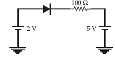
Question: Current through the ideal diode as shown in figure is
(a) zero
(b) 20 A
(c) 1 /20 A
(d) 1/50 A
Answer:
A
Question: In a half wave rectifier circuit operating from 50 Hz mains frequency, the fundamental frequency in the ripple would be
(a) 25 Hz
(b) 50 Hz
(c) 70.7 Hz
(d) 100 Hz
Answer:
B
Assertion & Reasoning Based MCQs
For question numbers 53-60, two statements are given-one labelled Assertion (A) and the other labelled Reason (R).
Select the correct answer to these questions from the codes (a), (b), (c) and (d) as given below.
(a) Both A and R are true and R is the correct explanation of A
(b) Both A and R are true but R is NOT the correct explanation of A
(c) A is true but R is false
(d) A is false and R is also false
Question: Assertion (A) : p-n junction diode can be used even at ultra high frequencies.
Reason (R) : Capacitative reactance of a p-n junction diode increases as frequency increases.
Answer:
C
Question: Assertion (A) : The conductivity of a semiconductor increases with rise of temperature.
Reason (R) : On rising temperature covalent bonds of semiconductor breaks.
Answer:
C
Question: Assertion (A) : The direction of diffusion current in a junction diode is from n-region to p-region.
Reason (R) : The majority current carriers diffuse from a region of lower concentration to a region of higher concentration.
Answer:
D
Question: Assertion (A) : The resistance of p-n junction is low when forward biased and is high when reverse biased.
Reason (R) : In reversed biased, the depletion layer is reduced.
Answer:
C
Question: Assertion (A) : The half-wave rectifier work only for positive half cycle of ac.
Reason (R) : In half-wave rectifier only one diode is used.
Answer:
A
Question: Assertion (A) : The resistivity of a semiconductor increases with temperature.
Reason (R) : The atoms of a semiconductor vibrate with larger amplitude at higher temperatures thereby increasing its resistivity.
Answer:
D
Question:Assertion (A) : In a semiconductor diode,the reverse biased current is due to drift of free electrons and holes.
Reason (R) : The drift of electrons and holes is due to thermal excitations.
Answer:
B
Question: Assertion (A) : The ratio of free electrons to holes in intrinsic semiconductor is greater than one.
Reason (R) : The electrons are lighter particles and holes are heavy particles.
Answer:
B
Case Based MCQs
Case I : Read the passage given below and answer the following questions from 36 to 40. Biasing of Diode When the diode is forward biased, it is found that beyond forward voltage V = Vk, called knee voltage, the conductivity is very high. At this value of battery biasing for p-n junction,the potential barrier is overcome and the current increases rapidly with increase in forward voltage. When the diode is reverse biased, the reverse bias voltage produces a very small current about a few microamperes which almost remains constant with bias. This small current is reverse saturation current.
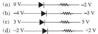
Question: In which of the following figures, the p-n diode is forward biased.
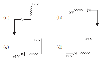
Answer:
C
Question: In the case of forward biasing of a p-n junction diode, which one of the following figures correctly depicts the direction of conventional current (indicated by an arrow mark)?
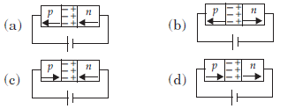
Answer:
D
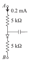
Question: If an ideal junction diode is connected as shown, then the value of the current I is
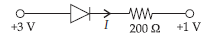
(a) 0.013 A
(b) 0.02 A
(c) 0.01 A
(d) 0.1 A
Answer:
C
Question: Based on the V-I characteristics of the diode,we can classify diode as
(a) bi-directional device
(b) ohmic device
(c) non-ohmic device
(d) passive element
Answer:
C
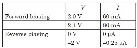
Question: The V-I characteristic of a diode is shown in the figure. The ratio of forward to reverse bias resistance is
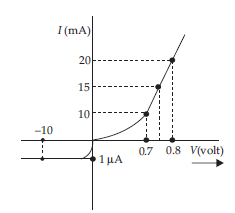
(a) 100
(b) 106
(c) 10
(d) 10–6
Answer:
D
p-n Junction Diode
A silicon p-n junction diode is connected to a resistor R and a battery of voltage VB through a milliammeter (mA) as shown in figure. The knee voltage for this junction diode is VN = 0.7 V. The p-n junction diode requires a minimum current of 1 mA to attain a value higher than the knee point on the I-V characteristics of this junction diode. Assuming that the voltage V across the junction is independent of the current above the knee point.
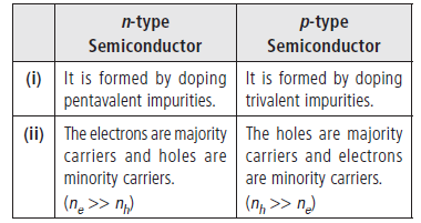
A p-n junction is the basic building block of many semiconductor devices like diodes. Important process occurring during the formation of a p-n junction are diffusion and drift. In an n-type semiconductor concentration of electrons is more as compared to holes. In a p-type semiconductor concentration of holes is more as compared to electrons.
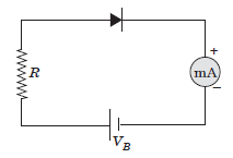
Question: If VB = 5 V, the maximum value of R so that the voltage V is above the knee point voltage is
(a) 40 kΩ
(b) 4.3 kΩ
(c) 5.0 kΩ
(d) 5.7 kΩ
Answer:
B
Question: Which of the below mentioned statement is false regarding a p-n junction diode?
(a) Diodes are uncontrolled devices.
(b) Diodes are rectifying devices.
(c) Diodes are unidirectional devices.
(d) Diodes have three terminals.
Answer:
D
Question: When the diode is reverse biased with a voltage of 6 V and Vbi = 0.63 V. Calculate the total potential.
(a) 9.27 V
(b) 6.63 V
(c) 5.27 V
(d) 0.63 V
Answer:
B
Question: If VB = 5 V, the value of R in order to establish a current to 6 mA in the circuit is
(a) 833 Ω
(b) 717 Ω
(c) 950 Ω
(d) 733 Ω
Answer:
B
Question: If VB = 6 V, the power dissipated in the resistor R, when a current of 6 mA flows in the circuit is
(a) 30.2 mW
(b) 30.8 mW
(c) 31.2 mW
(d) 31.8 mW
Answer:
D
Very Short Answer Type Questions
Question: What is the difference between an n-type and a p-type extrinsic semiconductor?
Answer:
Question: What is the function of a photodiode ?
Answer: Photodiode is used to detect the light signal and to measure light intensity.
Question: What happens to the width of depletion layer of a p-n junction when it is (i) forward biased, (ii) reverse biased ?
Answer: (i) Forward biased : As forward voltage opposes the potential barrier and effective barrier potential decreases. It makes the width of the depletion layer smaller.
(ii) Reverse biased : As reverse voltage supports the potential barrier and effective barrier potential increases. It makes thewidth of the depletion layer larger.
Question: In an n-type semiconductor, where does the donor energy level lies.
Answer: (b) : In n-type semiconductor, the donor energy level lies just below the conduction band.
Question: Name the junction diode whose I-V characteristics are drawn below :
Answer:The junction diode is solar cell.
Short Answer Type Questions
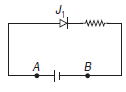
Question: A 3 V battery may be connected across the points A and B as shown. Assuming ideal diode, find the current supplied by battery if the positive terminal of the battery is connected to the point A.
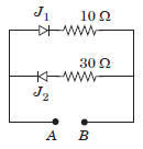
Answer: If A is positive and B is negative, J1 is forward biased and J2 is reverse biased, so effective current is
⇒ ia = = 0.3 A.
Question: Name the important process that occur during the formation of a p-n junction. Explain briefly, with the help of a suitable diagram, how a p-n junction is formed. Define the term ‘barrier potential’.
Answer: Two processes that take place in the formation of a p-n junction are diffusion and drift.
When p-n junction is formed, then at the junction, free electrons from n-type diffuse over to p-type, thereby filling in the holes in p-type. Due to this a layer of positive charge is built on n-side and a layer of negative charge is built on p-side of the p-n junction. This layer sufficiently grows up within a very short time of the junction being formed, preventing any further movement of charge carriers (i.e., electrons and holes) across the junction. Thus a potential difference V0 of the order of 0.1 to 0.3 V is set up across the p-n junction called potential barrier or junction barrier. The thin region around the junction containing immobile positive and negative charges is known as depletion layer
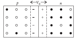
Question: The number densities of electrons and hole in pure Si at 27°C is 2 × 10¹⁶ m–3. When it is doped with indium, the hole density increases to 4 × 10²² m–3, find the electron density in doped silicon.
Answer: For extrinsic or doped semiconductor
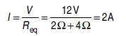
Question: The circuit shown in the figure has two oppositely connected ideal diodes connected in parallel. Find the current flowing through each diode in the circuit.
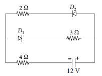
Answer: Diode D1 is reverse biased,so it offers an infinite resistance. So no current flows in the branch of diode D1.
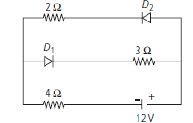
Diode D2 is forward biased, and offers negligible resistance in the circuit. So current in the branch
Question: Why photodiodes are required to operate in reverse bias ? Explain.
Answer: In reverse bias condition of photodiode, the change in saturation reverse current is directly proportional to the change in the incident light flux or light intensity, which can be measured accurately. It is not so when photodiode is forward biased.
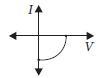
Question: Draw V-I characteristics of a p-n junction diode. Explain, why the current under reverse bias is almost independent of the applied voltage up to the critical voltage.
Answer:
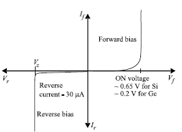
The reverse current is due to minority charge carriers and even a small voltage is sufficient to sweep the minority carriers from one side of the junction to the other side of the junction. Here the current is not limited by the magnitude of the applied voltage but is limited due to the concentration of the minority carrier on either side of the junction.
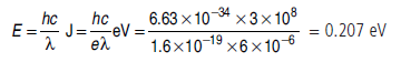
Question: Three photo diodes D1, D2 and D3 are made of semiconductors having band gaps of 2.5 eV, 2 eV and 3 eV, respectively. Which ones will be able to detect light of wavelength 6000 Å?
Answer: We know that, energy of incident photon E=hc/ λ
λ=6000 Å =600 nm (given)
E=1242eV nm/600 nm= 2.04 eV
D2 will detect these radiations because energy of incident radiation is greater than the band gap.
Question: (a) Mention the important considerations required while fabricating a p-n junction diode to be used as a light emitting diode (LED).
(b) What should be the order of band gap of an LED if it is required to emit light in the visible range?
Answer: (a) (i) There is very little resistance to limit the current in LED. Therefore, a resistor must be used in series with the LED to avoid any damage to it. (ii) The reverse breakdown voltages of LEDs are very low, typically around 5 V. So care should be taken while fabricating a p-n-junction diode so that the p side should only attached to the positive of battery and vice versa as LED easily get damaged by a small reverse voltage. (b) The semiconductor used for fabrication of visible LEDs must have at least a band gap of 1.8 eV because spectral range of visible light is about 0.4 mm to 0.7 mm, i.e., about 3 eV to 1.8 eV.
Question: A p-n photodiode is fabricated from a semiconductor with band gap of 2.8 eV. Can it detect a wavelength of 6000 nm?
Answer: Energy of the incident photon with a band gap of 6000 nm.
The photodiode need an energy of 2.8 eV to give response to incident light.
As E < Eg, the given photodiode cannot detect the radiation of wavelength 6000 nm.
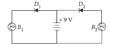
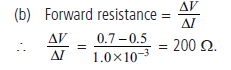
Question: (a) In the following diagram, which bulb out of B1 and B2 will glow and why?
(b) If the forward voltage in a semiconductor diode is changed from 0.5 V to 0.7 V, then the forward current changes by 1.0 mA. Find the forward resistance of diode junction.
Answer: (a) Bulb B1 will glow, as diode D1 is forward biased. Bulb B2 will not glow as diode D2 is reverse biased.
Long Answer Type Questions
Question: An a.c. signal is fed into two circuits ‘X’ and ‘Y’ and the corresponding output in the two cases have the waveforms as shown in figure.
(a) Identify the circuits ‘X’ and ‘Y’. Draw their labelled circuit diagrams.
(b) Briefly explain the working of circuit Y.
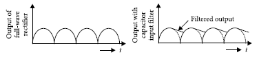
(c) How does the output waveform from circuit Y get modified when a capacitor is connected across the output terminals parallel to the load resistor?
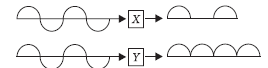
Answer: (a) X = Half wave rectifier
Y = Full wave rectifier
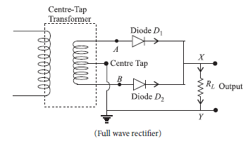
(b) Two p–n junction diodes can be used to make full wave rectifier which is used to convert alternating current into direct current
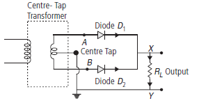
A full wave rectifier consists of two diodes connected in parallel across the ends of secondary winding of a center tapped step down transformer. The load resistance RL is connected across secondary winding and the diodes between A and B as shown in the circuit.
During positive half cycle of input a.c., end A of the secondary winding becomes positive and end B negative. Thus diode D1 becomes forward biased, whereas diode D2 reverse biased. So diode D1 allows the current to flow through it, while diode D2 does not, and current in the circuit flows from D1 and through load RL from X to Y.
During negative half cycle of input a.c., end A of the secondary winding becomes negative and end B positive, thus diode D1
becomes reverse biased, whereas diode D2 forward biased.
So diode D1 does not allow the current to flow through it but diode D2 does, and current in the circuit flows from D2
and through load RL from X to Y.
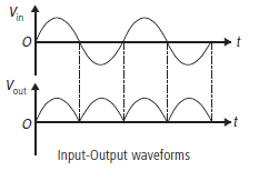
Since in both the half cycles of input a.c., electric current through load RL flows in the same direction, so d.c. is obtained across RL. Although direction of electric current through RL remains same, but its magnitude changes with time, so it is called pulsating d.c.
(c) A capacitor of large capacitance is connected in parallel to the load resistor RL. When the pulsating voltage supplied by the rectifier is rising, the capacitor C gets charged. If there is no external load, the capacitor would have remained charged to the peak voltage of the rectified output. However, when there is no load and the rectified voltage starts falling, the capacitor gets discharged through the load and the voltage across capacitor begins to fall slowly.
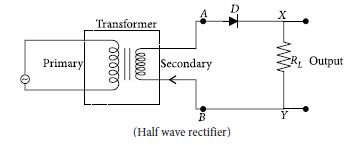
Question: Draw the circuit diagram of a p-n diode used as a half-wave rectifier. Explain its working.
Answer: Half wave rectifier:
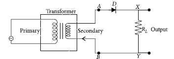
It consists of a diode D connected in series with load resistor RL across the secondary windings of a step-down transformer Primary of transformer is connected to a.c. supply. During positive half cycle of input a.c., end A of the secondary winding becomes positive and end B negative. Thus, diode D becomes forward biased and conducts the current through it. So, current in the circuit flows from A to B through load resistor RL.
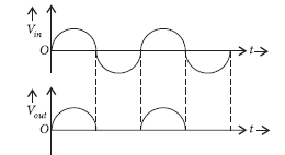

During negative half cycle of input a.c., end A of the secondary winding becomes negative and end B positive. Thus, diode D becomes reverse biased and does not conduct any current. So, no current flows in the circuit. Since electric current through load RL flows only during positive half cycle, in one direction only i.e., from A to B, so d.c. is obtained across RL.